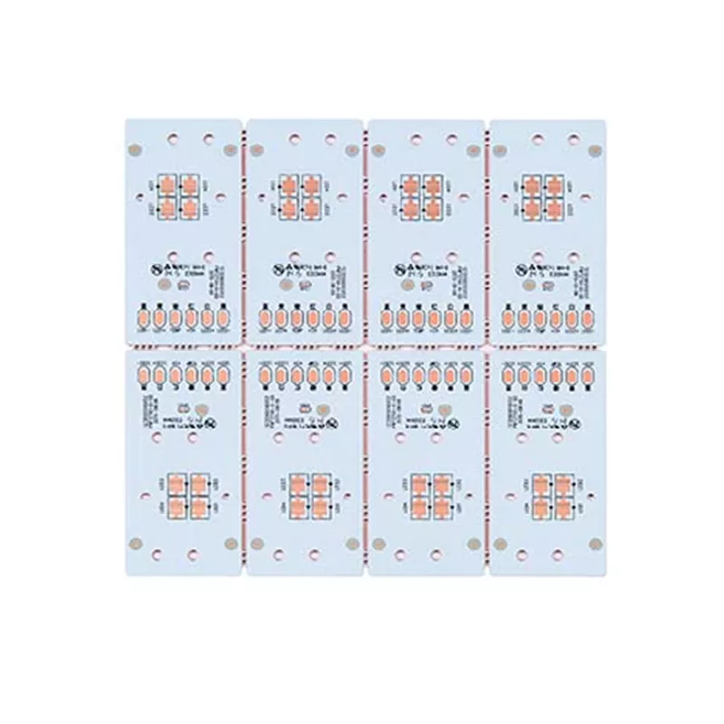
Thermoelectric separation metal based automotive PCB
Manufacturing characteristics of automotive PCB:
High frequency substrate
The car collision/predictive braking safety system functions as a military radar device. Due to the fact that automotive PCBs are responsible for transmitting microwave high-frequency signals, it is necessary to apply substrates with low dielectric loss together with ordinary substrate materials as PTFE. Unlike FR4 materials, PTFE or similar high-frequency substrate materials require special drilling and feed rates during the drilling process.
Thick copper PCB
Automotive electronic products bring more heat energy due to their high density and power. Hybrid and electric motors often require more advanced power transmission systems and more electronic functions, which leads to higher requirements for heat dissipation and high current.
Manufacturing thick copper double-layer PCBs is relatively easy, while manufacturing thick copper multi-layer PCBs is much more difficult. The key lies in the etching of thick copper images and filling of thickness gaps.
The internal paths of thick copper multilayer PCBs are all made of thick copper, so the pattern transfer photo induced dry film is relatively thick and requires great etching resistance. The etching time of thick copper patterns is long, and the etching equipment and technical conditions are in the best state to ensure the complete wiring of thick copper. When it comes to the manufacturing of external thick copper wiring, it is possible to first combine a relatively thick laminated copper foil and a patterned thick copper layer, and then perform film gap etching. The anti plating dry film of the graphic coating is also relatively thick.
The surface difference between the conductor and insulation substrate material in the thick copper multi-layer PCB and the ordinary multi-layer board stack is significant, and the resin is not completely filled and cavities are generated. To solve this problem, thin prepreg with high resin content should be coated as much as possible. The copper thickness of internal wiring on some multi-layer PCBs is uneven, and different pre impregnated materials can be applied to areas with large or small differences in copper thickness.
Previous: Ultra thick copper automotive PCB
Next: PCB half hole board


